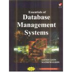
-
Your shopping cart is empty!


Digital Principles and System Design (AU R - 2017)
- ₹695.00
SHARE
This book Digital Principles and System Design provides the basic understanding of design and analysis of digital circuits with numerous solved problems.
- Cover
- About the authors
- Title Page
- Copyright Page
- Dedication
- Front Matter
- Contents
- Preface
- Acknowledgements
- UNITONE
- Chapter 1 Number System and Code
- 1.1 Introduction
- 1.2 Digital Signals
- 1.2.1 Why are Binary Numbers Used?
- 1.2.2 What is a Digital Signal?
- 1.3 Digital Computer and Digital System
- 1.4 Number Systems
- 1.5 Base Conversions
- 1.5.1 Binary to Decimal Conversion
- 1.5.2 Decimal to Binary Conversion
- 1.5.3 Decimal to Base-r
- 1.5.4 Base-r to Decimal
- 1.5.5 Binary to Octal and Binary to Hexadecimal Conversion
- 1.5.6 Conversion from Hexadecimal to Octal and Vice versa
- 1.6 Complements
- 1.6.1 r’s Complement or Radix Complement
- 1.6.2 (r–1)’s Complement or Diminished Radix Complement
- 1.6.3 Additional Method to Determine 10’s and 2’s Complements
- 1.7 Signed Binary Numbers
- 1.8 Binary Codes
- 1.8.1 Straight Binary Code or simply Binary Code
- 1.8.2 Gray Code
- 1.8.3 BCD Code [Binary coded decimal]
- 1.8.4 Excess-3 code
- 1.8.5 Error Detecting and Correcting Code
- 1.8.6 Hamming Code
- 1.8.7 Determination of Parity Bits
- 1.8.8 Single Error Correction and Double Error Detection
- 1.8.9 Alphanumeric Codes [ ASCII ]
- 1.8.10 Another Alphanumeric Code [ EBCIDIC ]
- 1.9 Binary Arithmetic
- 1.9.1 Binary Addition
- 1.9.2 Binary Subtraction
- 1.9.3 Binary Multiplication
- 1.9.4 Binary Division
- 1.10 2’s Complement/ 1’s Complement Arithmetic
- 1.10.1 Subtraction with 2’s Complements
- 1.10.2 Subtraction with 1’s Complement
- 1.10.3 BCD Addition/ Subtraction
- 1.10.4 Excess-3 Addition/ Subtraction
- Summary
- Review Questions
- Problems
- Chapter 2 DIGITAL CIRCUIT AND BOOLEAN ALGEBRA
- 2.1 Introduction
- 2.2 Basic Digital Circuits
- 2.2.1 AND Operation
- 2.2.2 OR Operation
- 2.2.3 NOT Operation
- 2.2.4 Nand and Nor Operations
- 2.2.5 NAND Operation
- 2.2.6 NOR Operation
- 2.2.7 Ex-OR and Ex-NOR Operations
- 2.3 Boolean Algebra
- 2.3.1 Basic Definitions
- 2.4 Basic Theorem and Properties of Boolean Algebra
- 2.4.1 Proof of Theorems
- 2.4.2 Postulate 4a Distributive law
- 2.4.3 Postulate 4b Distributive law
- 2.5 Boolean Function
- 2.6 Canonical and Standard Forms
- 2.6.1 Minterms and Maxterms
- 2.6.2 Sum of Minterms
- 2.6.3 Product of Maxterms
- 2.6.4 Conversion between Canonical forms
- 2.6.5 Standard forms
- 2.7 Other Logic Operations
- 2.8 Integrated Circuits
- 2.8.1 Examples of IC Gates
- 2.8.2 Levels of Integration
- 2.9 Introduction to Digital Logic Families
- 2.9.1 Bipolar Logic Families
- 2.9.2 Unipolar Logic Families
- 2.10 Brief Discussion of Popular Families
- 2.10.1 Transistor-Transistor Logic (TTL)
- 2.10.2 Emitter-Coupled Logic (ECL)
- 2.10.3 Metal Oxide Semiconductor (MOS) and Complementary Metal Oxide Semiconductor (CMOS)
- 2.10.4 Characteristics of Digital IC
- 2.10.5 Current and Voltage parameters
- Summary
- Review Questions
- Problems
- Summary
- Review Questions
- Chapter 3 SIMPLIFICATION OF BOOLEAN FUNCTION
- 3.1 introduction
- 3.2 the k-map method
- 3.2.1 Two and Three Variables Maps
- 3.2.2 Four Variable Map
- 3.2.3 Representation of Truth Table on K-map
- 3.2.4 Representation of SOP and POS form on K-map
- 3.3 Simplification of Logical Functions Using K-Map
- 3.3.1 Simplification Using Three Variable K-Map
- 3.3.2 Simplification Using Four Variable K-Map
- 3.4 Don’t Care Condition
- 3.5 Prime Implicants and Essential Prime Implicants
- 3.6 Five and Six Variable Maps
- 3.6.1 Five Variable Map
- 3.6.2 Six Variable Map
- 3.7 Variation of Maps
- 3.8 Nand and Nor Implementation
- 3.8.1 Realization of basic gates using NAND and NOR
- 3.8.2 Graphical Symbol
- 3.8.3 Two Level Implementation
- 3.8.4 Multilevel Realization
- 3.8.5 Wired Logic
- 3.9 The tabulation method or Quine-Mcclusky method
- 3.9.1 Determination of Prime Implicants in Tabulation Method
- Summary
- Review Questions
- Problems
- UNITTWO
- Chapter 4 COMBINATIONAL LOGIC CIRCUITS
- 4.1 Introduction
- 4.2 Analysis and Design Procedure
- 4.2.1 Analysis procedure
- 4.2.2 Design Procedure
- 4.3 Adders / Subtractors
- 4.3.1 Half Adder and Half Subtractor
- 4.3.2 Full Adder and Full Subtractor
- 4.3.3 Binary Parallel Adder
- 4.3.4 Binary Parallel Subtractor
- 4.3.5 Binary Adder/Subtractor
- 4.3.6 Look-ahead Carry Adder
- 4.3.7 Decimal Adder / Subtractor
- 4.4 Magnitude Comparator
- 4.4.1 One-bit Magnitude Comparator
- 4.4.2 Two-bit Magnitude Comparator
- 4.4.3 Four-bit Magnitude Comparator
- 4.5 Decoders and Encoders
- 4.5.1 Decoders
- 4.5.2 Three to Eight Line Decoder
- 4.5.3 BCD to Seven Segment Decoder
- 4.5.4 Encoder
- 4.5.5 Priority Encoder
- 4.6 Multiplexer
- 4.6.1 Boolean Function Implementation using MUX
- 4.6.2 Interconnection of Multiplexers
- 4.7 Demultiplexer
- 4.7.1 Expansion of DEMUX and Implementation of Boolean Function
- 4.8 Code Conversion
- 4.8.1 Binary to Gray Code and Gray Code to Binary Conversion – Direct Method
- 4.8.2 Binary to Gray Code and Gray code to Binary conversion – Conventional Method
- 4.8.3 Binary to BCD
- 4.8.4 BCD to Binary Conversion
- 4.8.5 Eight – bit BCD to Binary Conversion
- 4.8.6 BCD to Excess-3 Code Conversion
- 4.8.7 Excess-3 to BCD Code Converter
- 4.9 Parity Generator / Checker
- 4.9.1 Parity Generator
- 4.9.2 Parity Checker
- 4.10 Functionally Complete Set
- 4.11 Hardware Descriptive Language
- 4.11.1 Introduction
- 4.11.2 Verilog HDL
- 4.11.3 HDL for Combinational circuits
- Summary
- Review Questions
- Problems
- Chapter 5 FLIP-FLOPS
- 5.1 Introduction
- 5.2 A One-Bit Memory Cell
- 5.3 S-R Flip-Flop
- 5.3.1 S-R latch with NAND gate
- 5.3.2 NOR S-R Latch
- 5.3.3 Clocked S-R latch (S-R Flip-Flop)
- 5.3.4 Characteristic Equation
- 5.3.5 Timing Diagram
- 5.3.6 Preset and Clear
- 5.4 J-K Flip-Flop
- 5.4.1 Characteristic Equation
- 5.4.2 Timing Diagram
- 5.4.3 Race Around Condition
- 5.4.4 Master Slave Flip-flop
- 5.5 Delay Flip-Flop
- 5.5.1 Characteristic Equation
- 5.6 T flip-flop
- 5.6.1 Characteristic Equation
- 5.7 Flip-Flop Excitation Tables
- 5.8 Conversion of Flip-Flop From one Type to Another Type
- 5.9 Edge Triggered Flip-Flops
- 5.10 Edge Triggered S-R Flip-Flop
- 5.11 Applications of Flip-Flops
- Summary
- review questions
- Problems
- Chapter 6 SYNCHRONOUS SEQUENTIAL CIRCUIT
- 6.1 Introduction
- 6.2 Sequential Circuit Model
- 6.3 Terms and Definitions Used in Sequential Circuit
- 6.4 Analysis of Synchronous Sequential Circuits
- 6.4.1 Analysis Procedure
- 6.5 Synthesis Synchronous Sequential Circuit
- 6.5.1 Design Procedure
- 6.5.2 State Reduction
- 6.5.3 State Assignment
- Summary
- Review Questions
- Problems
- Chapter 7 REGISTERS AND COUNTERS
- 7.1 Introduction
- 7.2 Registers
- 7.2.1 Shift Registers
- 7.2.2 Serial in Serial Out [SISO] Shift Register
- 7.2.3 Serial in Parallel Out [SIPO] Shift Register
- 7.2.4 Parallel in Serial Out [PISO] Shift Register
- 7.2.5 Parallel in Parallel Out [PIPO] Shift Register
- 7.2.6 Bidirectional Shift Register
- 7.3 Universal Register
- 7.4 Applications of Shift Register
- 7.4.1 Ring Counter
- 7.4.2 Johnson Counter
- 7.5.1 Ripple Counter
- 7.5.2 UP / DOWN Counter
- 7.5.3 Three Bit Binary Ripple Counter
- 7.6 Modulus of Counter
- 7.6.1 Mod – 5 Counter
- 7.6.2 Mod – 10 Counter or Decade Counter
- 7.7 Synchronous Counter
- 7.7.1 Three Bit Synchronous Counter
- 7.7.2 UP / DOWN Counter
- 7.8 Design of Counter
- 7.9 Hdl for Sequential Logic Circuits
- Summary
- Review Questions
- Problems
- UNITFOUR
- Chapter 8 ASYNCHRONOUS SEQUENTIAL CIRCUIT
- 8.1 Introduction
- 8.2 Terms and Definitions Used in Asynchronous Sequential Circuit
- 8.3 Analysis of Asynchronous Sequential Circuit
- 8.3.1 Fundamental Mode Circuit without Latches
- 8.3.2 Circuit with Latches
- 8.3.3 Implementation of Sequential Circuit with SR Latch
- 8.4 Design of Asynchronous Sequential Circuit
- 8.4.1 Primitive Flow Table
- 8.5 State Reduction Techniques
- 8.5.1 State Reduction of Completely Specified States
- 8.5.2 State Reduction of Incompletely Specified States
- 8.6 State Assignment and Unspecified Output Assignment
- 8.6.1 Races and Cycles
- 8.6.2 Race Free State Assignments
- 8.6.3 Unspecified Output Assignment
- 8.7 Hazards
- 8.7.1 Circuits with Hazard
- 8.7.2 Hazard Free Circuit
- 8.7.3 Effect of Hazards in Asynchronous Sequential Circuit
- 8.7.4 Essential Hazards
- 8.8 Design Example
- UNITFIVE
- Chapter 9 memory and programmable logic device
- 9.1 Introduction
- 9.2 Random Access Memory – Ram
- 9.2.1 Basic Terms and definition
- 9.2.2 Memory Unit
- 9.2.3 Classifications of RAM
- 9.3 Memory Decoding
- 9.3.1 Coinciding Decoding
- 9.3.2 Address Multiplexing
- 9.4 Error Detection and Correction
- 9.4.1 Hamming Code
- 9.4.2 Single Error Correction and Double Error Detection
- 9.5 Read Only Memory – ROM
- 9.5.1 Architecture of ROM
- 9.5.2 Classification of ROM
- 9.5.3 ROM as a PLD
- 9.5.4 PLD Using Array Logic Diagram
- 9.6 Programmable Logic Array (Pla)
- 9.6.1 Structure of PLA
- 9.7 Programmable Array Logic [Pal]
- 9.8 Sequential Programmable Device
- 9.8.1 SPLD
- 9.8.2 CPLD
- 9.8.3 FPGA
- 9.9 Application Specific Integrated Circuit: Asic
- 9.9.1 Full-Custom ASIC
- 9.9.2 Standard Cell Based ASIC
- 9.9.3 Gate-Array-Based ASIC
- Summary
- Review Questions
- Problems
- Two Mark Questions and Answers
- Solved Question Papers
- May/June 2013
- Nov/Dec 2012
- May/June 2012
- Nov/Dec 2011
- April/May 2011
- Nov/Dec 2010
- April/May 2010
- Nov/Dec 2009
- May/ June 2009
- References
- Index
Sanjay Kumar Suman is currently Assistant Professor, Department of Electronics and Communication Engineering, Easwari Engineering College, Chennai. He has more than 9 years of teaching experience.
L Bhagyalakshmi is currently Assistant Professor, Department of Information Technology, Easwari Engineering College, Chennai. She has more than 8 years of teaching experience.
Reviews
There are no reviews for this product.

Management Information System
₹550.00
Modern approach to MIS treats it as an integrated management function reckons for the digital world...

Operating System
₹250.00
This book, Operating System, is crafted for students pursuing Computer Science, Computer Application..

Introduction to Information Systems
₹350.00
This book highlights the role and functioning of modern Information System (IS departments and their..

Operating Systems
₹395.00
This book Operating Systems by V. Sridhar is designed as per the Anna University syllabus for studen..
Essentials of Java Programming
₹450.00
Java the general purpose programming language is the choice programming language of professional pro..

Natural Language Processing
₹350.00
Natural Language Processing is a comprehensive textbook designed for students, researchers, andprofe..

Multi Core Architectures & Programming
₹495.00
This book has been designed to address the syllabi requirements of Anna University Regulations. It a..
Deep Learning Using Python
₹395.00
This book Deep Learning Using Python has been designed for undergraduate and postgraduate students o..

Python Programming
₹195.00
This book Python Programming Theory and Practical is designed to address the requirements of undergr..
Visual C#.Net
₹650.00
The .Net framework has a lot of advantage over the conventional programming architectures in terms o..

Visual Basic.Net
₹650.00
Visual Basic.Net, an object-oriented programming language implemented on .Net framework is the easie..
Advanced Computer Architecture 3e
₹495.00
This book Advanced Computer Architecture is designed for a one-semester advanced course targeted at ..

Problem Solving Using Python
₹250.00
This book Problem Solving Using Python is designed to address the requirements of undergraduate stud..